![]() ISSN 0798 1015
ISSN 0798 1015

![]() ISSN 0798 1015
ISSN 0798 1015
 Vol. 40 (Number 44) Year 2019. Page 2
MUÑOZ-GALEANO, Nicolás 1; LOPEZ-LEZAMA, Jesús M. 2 & VILLADA-DUQUE, Fernando 3
Received: 24/01/2019 • Approved: xx/12/2019 • Published 28/12/19
2. Proposed methodology for teaching the buck converter
ABSTRACT: This paper presents a methodology for teaching the buck converter with losses for the power electronics and related courses that can be used for academic purposes and a powerful tool of design. The methodology includes the design details and the stationary state analysis which permits to establish the gains of the system. There are also included efficiency and conduction modes analyses. There were deduced mathematical models that are also useful as a base for scientific papers, validated through simulation results. |
RESUMEN: Este artículo presenta una metodología para la enseñanza del convertidor reductor con pérdidas para el curso de electrónica de potencia y afines que puede usarse con propósitos académicos y como una potente herramienta de diseño. La metodología incluye el detalle del diseño que incluye el análisis del estado estacionario del convertidor que permite establecer las ganancias del sistema. También es incluido un análisis de la eficiencia y de los modos de conducción. Se deducen modelos que también sirven como base de artículos científicos que son validados mediante resultados de simulación. |

Most of the papers related with the design of buck converters make their contribution in the use of the model, not presenting enough attention in the deduction of the model. Details of the deduction of the model permit the understanding of the operating principle and also facilitate the design of the control structure.
Steady-state analysis of buck converter is useful since it is possible to observe the behavior of the converter in operation, so decisions can be taken from the design stage (Liuet al., 2007). Steady-state analysis receives a special attention of designers, being presented as a powerful tool in Liang and Tseng (2005). The deduction of the equations is not an easy task, so most designers prefer to skip the steady-state stage and proceed to the control stage, losing the opportunity to understand the behavior of the converter and making better decisions from the beginning of the design (Arango et al., 2013).
In general terms, losses should be taken into account to correctly predict the behavior in the entire operation range of the converter (Beldjajev, and Roasto, 2012; Davoudi et al., 2013). If losses are not included, the steady analysis is straightforward but does not correctly represent the behavior. Simplified models are not able to predict voltage gain and efficiency since they do not consider non-linearities (Galigekere and Kazimierczuk, 2012). Inductor and capacitors losses are usually modeled as series resistances (Geyer et al., 2008; Arango et al., 2013; Vlad et al., 2014). Some designing approaches take into account the losses resistances in inductors and capacitors (Geyer et al., 2008; Beldjajev and Roasto, 2012; Galigekere and Kazimierczuk, 2012; Davoudi et al., 2013). When these series resistances are included in the modeling, the equations obtained from the average model contain from the beginning the non-linearities.
Buck converters are widely used in industry. A development of a buck converter for photovoltaic applications is presented in Hasaneen and Elbaset (2008) and in Masri et al. (2012). Deekshitha and Shenoy (2017) presented the design and simulation of synchronous buck converter for LED application. Besides, Bi and Xia (2010) presented a modeling and simulation of dual-mode buck converter. Also, Alargt et al., (2017) designed an adaptive delta modulation controller for interleaved buck DC-DC converter. All these works have a steady-state analyses, nonetheless they do not include inductor and capacitor losses.
On the other hand, technical literature is mainly focus on control techniques for buck converters (Chen and Chen, 2008; Restrepo et al., 2013; Van der Broeck et al., 2015). Others are focused on the design for a particular application (Hasaneen, B. M. and Elbaset, A. A., 2008; Bi, Z. and Xia, W., 2010; Masri, S. et al., 2012; Alargt, et al., 2017; Deekshitha C. and Shenoy, K. L., 2017). Technical literature is focus on using the buck converter model for control or development purposes; nevertheless, there is not reported a procedure or methodology to obtain its model or operating principle. The objective of the work is to propose a methodology for teaching step by step the design of a buck converter that can be used for academic purposes and is presented as a powerful tool of design.
An understandable methodology for teaching the buck converter must at least include: 1) explanation of switching states and principle of operation, 2) deduction of the differential equations that govern the behavior of the converter, 3) application of average model to obtain the gains of the system to obtain the steady state of the converter, 4) deduction of the transformer model to obtain the efficiency, 5) deduction of the condition to operate in Continuous Condition Mode (CCM). Also, inductor and capacitor losses must be included to obtain a more realistic approximation of the converter. The proposed methodology is composed of five steps:
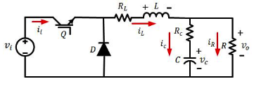
Buck converter function is to maintain a regulated output voltage lower than its input voltage; for this reason it is also known as the reducer converter. Figure 1 illustrates the equivalent circuit of the Buck converter. is the input voltage or source, while is the output voltage. The inductor () of the converter stores energy and then transfers it to the capacitor () and the load (). Power transistor () and diode () operate as switches. Diode must be of high speed to prevent that the switching frequency of the power transistor affects its activation time. represents the losses of the inductor, while represents the losses of the capacitor. and are included in the equivalent circuit to obtain a more realistic modeling of the system.
Figure 1
Equivalent circuit of a buck converter
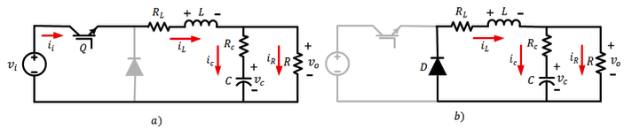
The converter has two switching states according to the position of Q: a) closed and b) open (Figure 2). When is closed (Figure 2a), the diode is reverse polarized, that is, it is open. In this state, the inductor is in series with and the current flows from the input source to the capacitor, charging the inductor while the capacitor supplies power to the load. In this switching state, the current in the inductor increases. When the switch is open (Figure 2b), the source does not feed the converter, the inductor changes its polarity and prevents a sudden change in the inductor current, also the diode is directly polarized and the energy stored in the inductor is transferred to the load and the capacitor through . Passive law of signs should be established to obtain polarities (reference voltages) and senses of currents (reference currents).
Figure 2
States of buck converter: a) closed, b) open
For writing the differential equations that govern the behavior of the converter, firstly the differential equations for each switching state must be written. Kirchhoff Laws of voltage and current are used taking into account voltage and current references that were established in step 1. It is very important to use the references for writing because, if they are not used, the model would not be coherent. Equations (1) and (2) are the differential equations that govern the behavior when the switch is closed, while equations (3) and (4) are the differential equations operating when the switch is open.
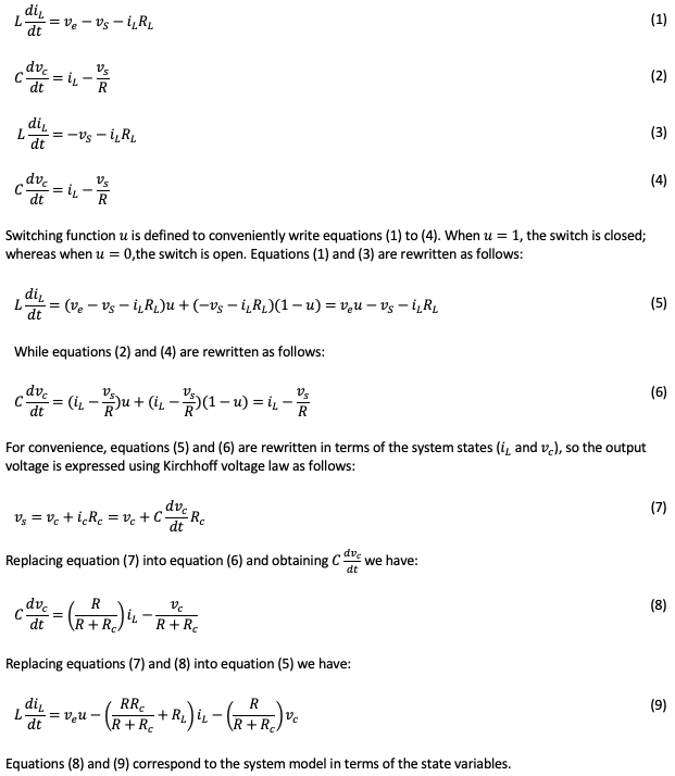
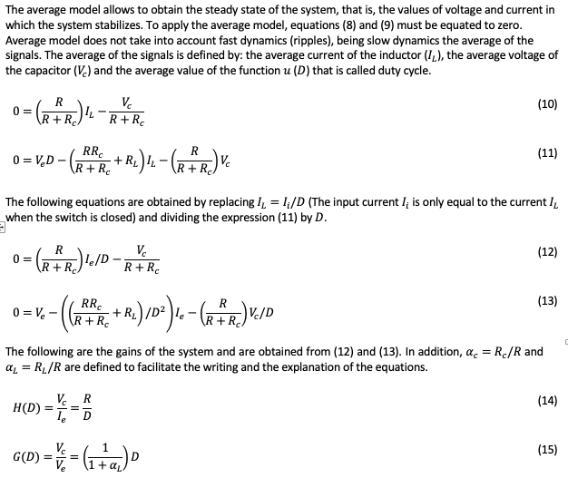
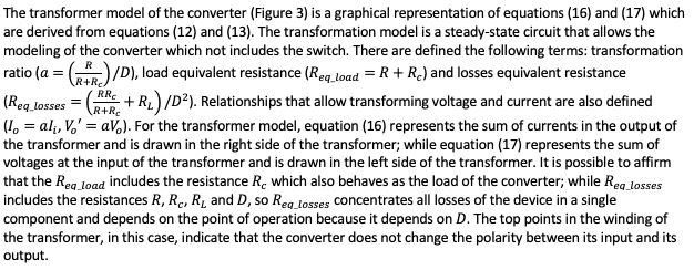
Figure 3
Transformer model of buck converter
Figure 4
Graphical representation of CCM
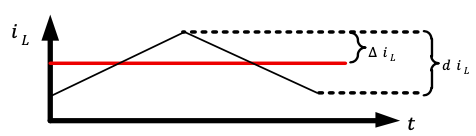
Figure 5
Gain of voltage for buck converters
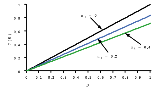
Figure 6
Efficiency for different values of αL and αc
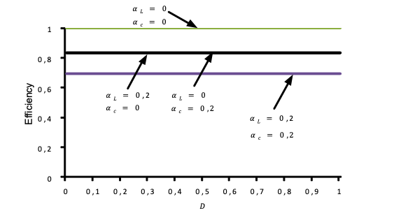
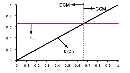
Fig 7
CCM condition for the buck converter
This paper presented a methodology for teaching the design of a buck converter with five steps that permits the understanding of its operating principle and main particularities. All equations were carefully organized to ensure that the reader can follow a step by step deduction of equations which facilitates their understanding.
Step one established the switching states; so polarities of voltages and direction of currents were obtained, being possible to establish voltage and current references as well as the buck converter principle of operation.
Step two, following Kirchhoff laws for each switching state, presented the deduction of the differential equations that govern the behavior of the converter. Equations were conveniently written using a switching function.
Step three used the average model to obtain the gains of the system. This allows to establish the steady state of the system, that is, the values of voltage and current in which the system stabilizes.
Step four presented the transformer model to obtain the efficiency of the converter. Average model were conveniently drawn to better explain the efficiency concept, relationship between the input and output powers were shown using an equivalent circuit that includes power losses.
Step five deduced the condition to operate in CCM. An inequality equation was deduced to easily establish the limit in which the converter operates in CCM.
Simulation results consolidated the acquired concepts during the methodology showing the variations of voltage gain and efficiency when losses are changed. Also, CCM limit was clearly shown in a figure to reinforce such concept, so it was possible to define the operating range of the converter.
The authors want to acknowledge Universidad de Antioquia for its support through the project“estrategia de sostenibilidad”.
Alargt, F. S., Ashur, A. S., and Kharaz, A. H. (2017). Adaptive delta modulation controller for interleaved buck DC-DC converter. 52nd International Universities Power Engineering Conference (UPEC), Heraklion (Greece),1-6.
Arango, E., Ramos-Paja, C. A., Calvente, J., Giral, R., and Serna-Garces, S. I. (2013). Asymmetrical Interleaved DC/DC Switching Converters for Photovoltaic and Fuel Cell Applications - Part 2: Control-Oriented Models. Energies, 6(10), 5570-5596.
Beldjajev, V. and Roasto, I. (2012). Efficiency and Voltage Characteristics of the Bi-Directional Current Doubler Rectifier. Przeglad Elektrotechniczny, 88(8), 124–129.
Bi, Z. and Xia, W. (2010). Modeling and Simulation of Dual-Mode DC/DC Buck Converter. Second International Conference on Computer Modeling and Simulation, Sanya, Hainan (China), 371-375.
Chen, S. and Chen, J. (2008). Study of the Effect and Design Criteria of the Input Filter for Buck Converters With Peak Current-Mode Control Using a Novel System Block Diagram. IEEE Transactions on Industrial Electronics, 55(8), 3159-3166.
Davoudi, A., Jatskevich, J., Chapman, P. L. and Bidram, A. (2013). Multi-Resolution Modeling of Power Electronics Circuits Using Model-Order Reduction Techniques. IEEE Transactions on Circuits and Systems I: Regular Papers, 60(3), 810–823.
Deekshitha C. and Shenoy, K. L. (2017). Design and simulation of synchronous buck converter for LED application. 2nd IEEE International Conference on Recent Trends in Electronics, Information & Communication Technology (RTEICT), Bangalore (India), 142-146.
Galigekere, V. P. and Kazimierczuk, M. K. (2012). Analysis of PWM Z-Source DC-DC Converter in CCM for Steady State. IEEE Transactions on Circuits and Systems I: Regular Papers, 59(4), 854–863.
Geyer, T., Papafotiou, G., Frasca, R. and Morari, M. (2008). Constrained Optimal Control of the Step-Down DC-DC Converter. IEEE Transactions on Power Electronics, 23(5), 2454–2464.
Hasaneen, B. M. and Elbaset Mohammed, A. A. (2008). Design and simulation of DC/DC boost converter. 12th International Middle-East Power System Conference, Aswan (Egypt), 335-340.
Liang, T. J. and Tseng, K. C. (2005). Analysis of integrated boost-flyback step-up converter. IEE Proceedings - Electric Power Applications, 152(2), 217–225.
Liu, J., Hu, J. and Xu, L. (2007). Dynamic Modeling and Analysis of Z Source Converter -- Derivation of AC Small Signal Model and Design-Oriented Analysis. Power Electron. IEEE Trans., 22(5), 1786–1796.
Masri, S., Mohamad, N. and Hariri, M. H. M. (2012). Design and development of DC-DC buck converter for photovoltaic application. International Conference on Power Engineering and Renewable Energy (ICPERE), Bali (Indonesia), 1-5.
Restrepo, C., Konjedic, T., Calvente, J., Milanovic, M. and Giral, R. (2013). Fast Transitions Between Current Control Loops of the Coupled-Inductor Buck–Boost DC–DC Switching Converter. IEEE Transactions on Power Electronics, 28(8), 3648-3652.
Van der Broeck, C. H., De Doncker, R. W., Richter, S. A. and Bloh, J. V. (2015). Unified Control of a Buck Converter for Wide-Load-Range Applications. IEEE Transactions on Industry Applications, 51(5), 4061-4071.
Vlad, C., Rodriguez-Ayerbe, P., Godoy, E. and Lefranc, P. (2014). Advanced control laws of DC-DC converters based on piecewise affine modelling. Application to a stepdown converter. IET Power Electronics, 7(6), 1482–1498.
1. Docente e investigador del Grupo GIMEL. Departamento de Ingeniería Eléctrica. Universidad de Antioquia. Ingeniero electricista y doctor en Ingeniería Electrónica. Email: nicolas.munoz@udea.edu.co
2. Docente e investigador del Grupo GIMEL. Departamento de Ingeniería Eléctrica. Universidad de Antioquia. Ingeniero electricista y doctor en Ingeniería Eléctrica. Email: jmaria.lopez@udea.edu.co
3. Docente e investigador del Grupo GIMEL. Departamento de Ingeniería Eléctrica. Universidad de Antioquia. Ingeniero electricista y doctor en Ingeniería Eléctrica. Email: fernando.villada@udea.edu.co
[Index]
revistaESPACIOS.com

This work is under a Creative Commons Attribution-
NonCommercial 4.0 International License